Copyright Interesting Engineering
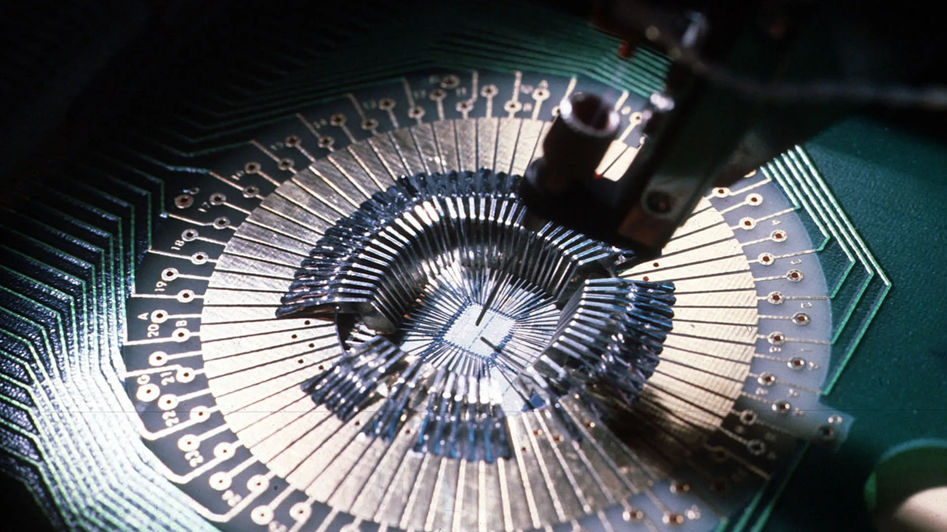
Chinese researchers have unveiled a new “fancy tool” that can pinpoint the source of manufacturing flaws during microchip production. According to the team, the new technology can cut errors by as much as 99%, marking a significant leap forward for domestic semiconductor production. At present, one of the most delicate steps in making computer chips is photolithography. This, basically, involves using light to “print” incredibly tiny circuit patterns onto silicon wafers. You can liken this process to developing a kind of microscopic photograph. During this process, lithography devices spread a photoresist (a light-sensitive liquid) over the silicon wafer. Following this, ultraviolet light is shone through a patterned mask, which acts as the “blueprint” of the circuit. After this, lithography machines chemically develop the photoresist so that some areas dissolve and others stay. What’s left acts as a protective stencil for later steps, like etching the metal or silicon. As efficient as this process is, it can lead to some serious issues over time. For example, during the development stage, the photoresist doesn’t always behave nicely. Some of the dissolved material clumps together into microscopic particles that can re-stick to the wafer. These particles cause defects, like bridges, breaks, or rough edges, that ruin chips. At 5-nanometre or smaller nodes (current cutting-edge chips), a tiny 30-nanometre particle (about 1/3,000th the width of a hair) can ruin a circuit and make the chip unusable. That can translate into big losses. Until now, manufacturers couldn’t see exactly what was happening inside that developer liquid; it was basically a black box. To this end, Professor Peng Hailin’s team from Peking University, Tsinghua, and HKU used a cryo-electron tomography (cryo-ET) technique to literally freeze the chemical process mid-action and look inside it in 3D. Cryo-ET is a process usually reserved in biology to study cells in minute detail. Using this, the team, after exposing and developing a wafer, rapidly froze the developer to 32°F (–175°C), stopping everything in place. They then used electron tomography, which takes many angled images and reconstructs a 3D view at the molecular level. This allowed them to watch how the photoresist polymers actually behave during development. Following this treatment, the team found that for the first time, they could see what was going wrong. For example, they discovered that photoresist molecules tangle together (like spaghetti) through weak hydrophobic interactions. These tangles grow into 30–40 nm particles. A breakthrough for Chinese semiconductors They also found that about 70% of these molecules don’t dissolve properly; they hang out at the air-liquid interface instead. When the wafer is rinsed, these clumps redeposit onto the surface, causing the defects. Based on those findings, the team came up with two simple but powerful fixes that are both compatible with existing chip fabrication techniques. They proposed slightly raising the bake temperature after exposure to reduce how much the polymers can tangle up. When implemented, they found that far fewer clumps form in the first place. The team also changed the development rinse process to trap polymers at the air-liquid interface. To this end, they altered the flow sweeps them away before they can reattach to the wafer. When they tested it, defect counts on 12-inch (30.5 cm) wafers dropped by over 99%, effectively achieving near-perfect lithography quality.