Copyright scmp
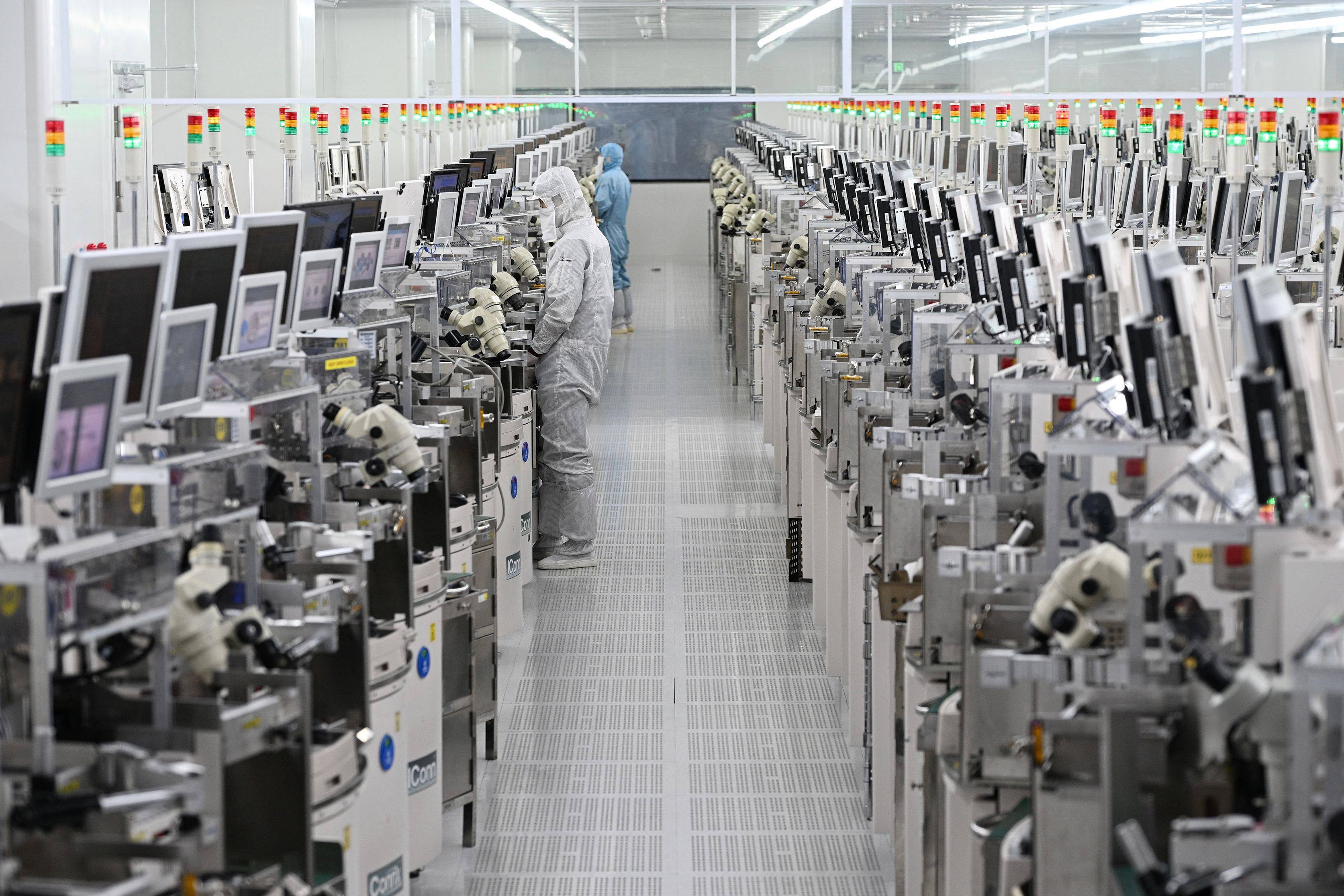
Chinese researchers claim to have achieved a key breakthrough in lithography technology in the latest step in the country’s effort to achieve self-sufficiency with advanced chips. A group of scientists from Peking University, along with other collaborators, made a breakthrough in visualising the molecular behaviour of photoresist, a light-sensitive material used in chipmaking, according to a paper published in top scientific journal Nature. The advance could lead to a significant reduction in defects in advanced chip manufacturing, they said. Photoresist, used in processes such as photolithography and photoengraving that involve forming a patterned coating on a surface, is a key input in chip manufacturing. China’s reliance on imported photoresist material is one factor restricting its advanced chip-production capabilities. The paper, first reported by the state-backed Science and Technology Daily on Friday, was touted by the newspaper as a step to solve “a key bottleneck hindering yield improvement” in advanced processes at 7 nanometres and below. The breakthrough is seen as a boost to China’s self-sufficiency, as lithography remains one of the biggest chokepoints. The world’s leading chip equipment supplier, ASML, has been banned from selling its most advanced extreme ultraviolet (EUV) lithography machines to China since 2019 under pressure from the US. “Despite decades of research, the microscopic behaviours of photoresist in liquid film and at interfaces remain elusive”, the researchers said, adding that this made defect control “largely a trial-and-error process”. Liquid film is the medium for the dissolution of photoresist to create nanoscale circuit patterns in lithography. The team used a “cryo-electron tomography” methodology to unravel the nanostructures of photoresist polymers in liquid film and at gas-liquid interfaces, according to the paper. This enabled them to eliminate contaminations across 12-inch wafers under industrial conditions, yielding a more than 99 per cent improvement in minimising pattern defects for fab-compatible lithography, the researchers said. The new methodology would advance defect control and improve yield in key processes such as lithography, etching and wet cleaning in advanced chip manufacturing, said Peng Hailin, a physical chemistry professor at Peking University and leader of the team, in the state-backed newspaper’s report. At the WeSemiBay Semiconductor Ecosystem Expo held in the southern tech hub Shenzhen earlier this month, Skyverse Technology, a materials subsidiary of local government-backed chip equipment maker SiCarrier, presented a photoresist that could be used for EUV production, according to a report by Taiwanese media outlet Digitimes. Still, China has been relying heavily on imports for photoresist, with more than 90 per cent of the material being sourced internationally, according to a report by China Chemical Market Insights in December. A few Japanese companies, including JSR, Tokyo Ohka Kogyo, Shin-Etsu Chemical and Fujifilm Electronic Materials, dominate the supply of high-end semiconductor photoresist.