Copyright XDA Developers
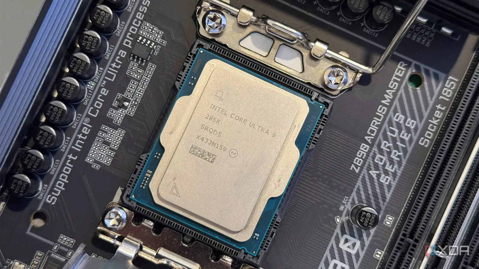
The next big leap in CPU design won’t come from adding more cores, chasing smaller nodes, or stacking additional chiplets onto one CPU. That's not to say that things like AMD's 3D V-Cache aren't good, meaningful innovations, but it doesn't really change how we think about CPUs. Backside power delivery, however, is the one CPU innovation that I'm actually really looking forward to. It's the sort of change that can reshape what's possible in terms of raw performance, cooling, and efficiency, not just for the enterprise market, but for PC builders and enthusiasts as well. What backside power delivery actually is Where your CPU gets its power from matters At its simplest, backside power delivery means moving the power delivery network (PDN) from the top side of the silicon die, to the underside. This power delivery network is essentially a collection of metal layers and vias that feed electricity to transistors. Traditionally, this has been located on the same side as the data I/O, which has forced engineers to make trade-offs for performance and efficiency. Routing power competes with logical signals, and any congestion there can lead to resistance and voltage droop, ultimately limiting density. By flipping the power delivery to the other side, these trade-offs are much less relevant. The front side can be entirely signal outing and transistors, while the back side can deliver power. This has been experimented with by the likes of IMEC and TSMC in lab chips for a while, but Intel's PowerVia PDN was the first implementation of backside power delivery meant to hit commercial chips, and while its initial debut was supposed to come with the Intel 20A node, which was skipped as a consumer platform. That doesn't mean we won't see PowerVia in the near future, though. Intel's Panther Lake architecture featuring PowerVia, built on Intel 18A, is set to release in laptops in January 2026. While the Arrow Lake desktop refresh that's coming won't feature BSPD, the Nova Lake desktop CPUs coming in late 2026 may feature the technology. It's yet to be seen if these chips are manufactured on Intel 18A, however. Why this matters Consumer chips will reap the benefits of this immediately Power delivery is one of those behind-the-scenes bottlenecks that most PC enthusiasts never think about, but it quietly defines how far a CPU can scale. When every watt that a processor uses has to travel downward, potentially disturbing logical signals, adding resistance and delay. This is why some high-end chips can run into voltage-stability limits long before they hit thermal ones. Technologies like PowerVia reduce what's known as IR drop, which is the loss of voltage along the route the power takes to its destination. This greater efficiency means transistors operate at their designed voltages more consistently, delivering more stable clocks. Intel's own testing saw a 6% increase in clock speeds and 30% voltage droop improvement on the same process node with the same voltage, but with the power delivery moved to the underside. The cooling advantage is also clear: moving the power delivery to the backside leaves the logic to make great contact with the IHS, where your CPU cooler then will have direct contact. In theory, this would help simplify CPU cooling and lessen the effects of voltage spikes on cooling under load. Backside power also plays nicely with future stacking technologies. Today’s 3D V-Cache and chiplet architectures rely on through-silicon vias and specialized bonding layers. With the top of the CPU freed from its power grid, we could see true logic-on-logic stacking, not just extra cache. This could be in the form of a CPU core layer directly bonded to an AI accelerator or an integrated GPU without the need for a separate substrate. Why it excites me more than process shrinkage We're reaching the physical limits of silicon As process nodes continue to shrink, the cost of producing a viable wafer goes way up, and in turn, that cost is passed down onto the consumer. On top of that, we've reached the limits of what silicon can do: gate lengths are measured in the tens of atoms. In other words, the huge gains we saw throughout the 2000s and into the 2010s aren't there anymore in the 2020s, it's largely going to be in technologies like backside power delivery to help increase density and efficiency, alongside new transistor designs like GAAFET and RibbonFET. Cleaner power delivery can mean more stable overclocks and undervolts, fewer transient spikes that cause crashes or throttling, and more consistent thermal behavior on top of that ~6% performance gain we see from moving power delivery. This could make a huge difference in CPU performance It's not as tangible as core counts, completely new architectures or AI accelerators, but backside power delivery is a genuinely meaningful step forward in modern chip design. It's about rethinking the physical limits of how power moves through your CPU, and that's the kind of change that could enable other innovations.