Copyright int10h
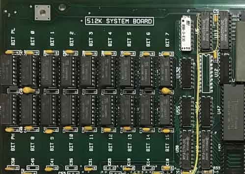
Something intriguing turned up recently over at the Vintage Computer Federation Forums. Member GearTechWolf occasio-nally rescues and dumps random ROM chips that show up on eBay, and makes the contents available so they aren't lost to the ages. One of his hauls turned up two pairs of EPROMs labeled "IBM" in plain dot-matrix: one showing part numbers (and "© IBM CORP 1981,1985"), the other tagged with a specific date ("25/05/90"). They came with no further identi-fication, and no hints about their origins, or what machines they may have come from. And just to establish that proper setting of suspense and mystery, neither pair could be content-matched against any known IBM firmware. Much poking and prying commenced. I didn't delve very deeply into the '25/05/90' odd/even pair, but it seemed to be some sort of PS/2 BIOS: it proved to contain those tell-tale extra VGA fonts (on which past verbiage abounds), and to share some other bits and pieces with known Model 35 SX/40 SX ROMs. Seeing that, I prodded the Ardent Tool crew, and Major Tom identi-fied it as rev. 2 of the 35-/40-SX firmware - earlier than other known variants. It's now up for download on the System ROMs page. The more intriguing one for me was the '1981, 1985' duo (yellow labels in the photo). A cursory look in a hex viewer revealed the following: EPROM 6448246 has the even addresses, 6448238 the odd addresses. The internal part numbers are 6480442 and 6480441, respectively. The BIOS date stamp in the standard location (F000:FFF5) is 03/08/85. At F000:330A, there's yet another date stamp - 02/14/85. The model byte (in the second-to-last position) is FCh. In 1985, the FCh model byte could only mean the 5170 (PC/AT),1 and the even/odd byte inter-leaving does point at a 16-bit bus. But there are three known versions of the PC/AT BIOS released during the 5170 family's lifetime, corres-ponding to the three AT mother-board types. This one here is clearly not one of them: its date stamps and part numbers don't match, and the actual contents are substan-tially different besides. My first thought was that this may have come from one of those more shadowy members of the 5170 family: perhaps the AT/370, the 3270 AT/G(X), or the rack-mounted 7532 Industrial AT. But known examples of those carry the same firmware sets as the plain old 5170, so their BIOS extensions (if any) came in the shape of extra adapter ROMs. Whatever this thing was - some other 5170-type machine, a prototype, or even just a custom patch - it seemed I'd have to inquire within for any further clues. The PC/AT BIOS: Known Versions This was a good time to brush up on the three official revi-sions of the AT BIOS: how to tell them apart, and how they corres-pond to hardware options. The following table was compiled mostly from the pages at Minus Zero Degrees (IBM 5170 BIOS Revisions) and PC DOS Retro (IBM PC BIOS version history), and from the info in Ralf Brown's Inter-rupt List. Where the sources weren't in total agree-ment, I went with what seemed to conform with IBM's pub-lished source code listings. That's the low-down on what we have to compare against. In this yet-unknown revision, both of the date stamps within the BIOS image (03/08/85 and 02/14/85) place it in-between revisions 1 and 2. So for the sake of conve-nience (read: laziness), I'll be stun-ningly original and refer to it below as "rev. 1.5". Are You AT Enough? Before I embarked on some actual reverse-enginee-ring, I thought I'd try a little experiment first: how would 86box's IBM AT emulation fare with this firmware? Easy enough to find out; just substitute these two ROM images for the expected even/odd pair (86box uses the rev. 3 BIOS by default) and see what happens. Since I don't have an actual IBM 5170, that's as close to an "AT compatibility test" as I could get, but this firmware appeared to pass muster: Our 'rev. 1.5' BIOS makes it through POST with no issues. The IBM AT Advanced Diagnostics v2.07 disk loads up, and dutifully reports the firmware's P/N and date string; System Checkout (which lists the installed hardware) and the SETUP procedure (which is where you configure it) both run as expected. Evidently this is some manner of PC/AT BIOS, or close enough to make Diagnostics happy. Poking at it under an emulator isn't going to tell us a whole lot more than this, however: we don't know exactly what this revision assumes about the hardware, so we can't expect to tell compati-bility issues from configuration errors, or just sketchy emulation. At this juncture (if you'll excuse the imagery) we might as well roll up our sleeves and start rummaging through the entrails. For more detailed notes about the disassembly itself, have a look at the repository. I'll just mention that the goal was to figure out just where and how this 'rev. 1.5' BIOS differs from the others, and this would have been much more difficult if it wasn't for two things: The published source listings for all official AT BIOS versions, from the respective editions of the PC/AT Technical Reference - available on Bitsavers (and on the Internet Archive: #1, #2, #3). The excellent reconstructions of the source code by Vernon Brooks over at PC DOS Retro, which have the listings in plain text (and they can be success-fully reassem-bled, too). I didn't go quite as far as trying to recon-struct a version that actually builds, but thanks to the above I believe I have things mostly figured out, so here's my analysis. The Code Base Just to get this out of the way, this is very clearly not a custom patch, or a little localized modifi-cation. Most obviously, all offsets/addresses differ from the other versions, and not just by a simple, easily-explained shift. The exceptions are certain entry points and tables (mostly in the top 4 KB) delibe-rately forced to fixed addresses, something that's been done in every PC-family BIOS.2 In fact, with some (important) diffe-rences which will be detailed below, overall the code base appears to be something you'd expect if you were looking at a snapshot of some interim state between rev. 1 and 2. Some sections are closer to their rev. 1 counter-parts, others to rev. 2; many contain elements of both, or follow the general logic of one version while still showing certain practices more common in the other. For instance, a routine may perform essentially the same thing it did in rev. 1, but include certain optimi-zations which are mostly found only in rev. 2, such as imme-diate multi-bit shifts (you might see SHL BL, 2 in place of two SHL BL, 1 instruc-tions),3 or updating segment registers with PUSH/POP (instead of MOVing the value through a go-between). Other routines appear more or less in the same form they have in rev. 2, while signs of the rev. 1 coding style still persist. For example, all the I/O required to access CMOS memory is done inline, as opposed to rev. 2 which calls two new routines for this purpose (CMOS_READ and CMOS_WRITE). Or the encoding of jumps: two-byte (short) jumps are often found padded with a NOP instru-ction, like in rev. 1, something that no longer happens in the later itera-tions.4 The more interesting parts, of course, are the sections which are unique to 'rev. 1.5' and don't have direct counter-parts elsewhere, but I'll be getting to them in a bit. Those aside, the whole thing does look like an authentic version of the BIOS code, caught in some interme-diate state of develop-ment between revisions 1 and 2 - including some (but not all) of the changes that later made it to the second revision, as well as a few modifi-cations that didn't. Top-Level Organization (and Build Environment) The other editions of the AT BIOS were all generated from multiple source files. Here we only have the final image, but by comparing the overall structure against the other versions, we can deduce the break-down into separate source modules. The arrange-ment of the code and data here is the same as in rev. 1, which suggests that 'rev. 1.5' was built before the restruc-turing that can be seen in the second revision. Rev. 1 was appa-rently assem-bled with MASM v1.0, but rev. 2 switched to v2.0, as we're told by the page titles in IBM's source listing. If the struc-tural overhaul was down to that change, then '1.5' was likely still built with MASM v1.0... a form of cruel and unusual punish-ment if there ever was one, but perhaps they had some inside scoops from Microsoft on how to deal with all the errata in that famously bug-infested mess of an assem-bler. Functionality (and Hardware Support) Comparison Now for some of the actual simila-rities and diffe-rences between 'rev 1.5' and its older/younger siblings. The code may be closer to the first revision in its general structure, but if we take the date stamps at face value, it post-dates rev. 1 by more than a year - while the next revision was only three or four months away. So it wasn't a complete surprise to find quite a few similarities with rev. 2. For instance, It supports 720K (3.5" DSDD) floppy disks, offi-cially intro-duced only in rev. 2. 21 different hard drive types are avai-lable: 01-14 and 16-22, just one short of rev. 2 (and 3), which add drive type 23. Only types 01-14 were recog-nized in rev. 1 (15 is always reserved). It implements INT 15h function C0h ("Get System Configuration"), which didn't exist in rev. 1, but was present in rev. 2 (and in all later PC compa-tible BIOSes). Keyboard support is more or less the same as in rev. 2: only the 84-key AT keyboard is (fully) supported, but some code for the 101/102-key Enhanced Keyboard is already present. The hardware IRQ handler (INT 09h) attempts to detect it, and uses its expanded scan code tables, but the enhanced INT 16h services are not available.5 In certain other respects, however, there's more in common with the first revision: It doesn't attempt to verify the 286's clock speed, a test that was added to POST in revisions 2 and 3 (at checkpoint 11h).67 When testing the floppy/hard drive controller ("combo card" in IBM-speak), it won't throw up a "601 diskette error" if it cannot find the "multiple data rate capa-bility" indi-cation bit. What this means in practice is that more third--party cont-rollers should be supported. POST checkpoint codes 02 and 03 mean the same things as in rev. 1 (respectively, these tests verify the CMOS Shutdown Byte and the BIOS ROM checksum). The later revisions swap these two tests around.6 Then you've got those peculiar sections where 'rev. 1.5' does its own thing entirely. The most signifi-cant ones handle RAM testing and parity errors: this also provides our biggest clue about just what sort of AT this firmware came from, so I'll expand on this down below. For now, just a few notes about some of the above: The System Configuration Table This is where we find the machine ID bytes: model, sub-model, and revision level. A pointer to this table is returned by the (new) BIOS function INT 15h/AH=C0h. Per RBIL, this was avai-lable in the PC XT since the 1986/01/10 BIOS, in the PC/AT since 1985/06/10 (second revision), and in all subsequent PC and PS/2 machines; but evidently 'rev. 1.5' had it first. The odd part is that it returns sub-model 01 and revision level 00, which is the same as the third revision BIOS - the second revision has sub-model 00, revision level 01. Perhaps the meaning (or the order) of these bytes was still not quite final at this point. On the other hand, the fourth ('feature') byte is 70h, like in rev. 2 and 3. Floppy Drive Support This is one area where the 'rev 1.5' code base diverges from all other revisions, but the actual functio-nality doesn't seem to be too diffe-rent from rev. 2. It looks more as if 3.5" 720 KB media support was shoe-horned into the rev. 1 code (which only handled 1.2 MB and 360 KB disks and drives). This somewhat over-compli-cated the logic of many routines, especially those dealing with state/format bits and varia-bles in the BIOS Data Area whose formats couldn't be changed, for the sake of compati-bility. Rev. 2 refactored and simpli-fied the floppy code, in part by imple-menting what the comments call a "new archi-tecture", along with two routines (XLAT_NEW and XLAT_OLD) which convert such data fields to a new internal format when entering a BIOS function, then back to the old format on exit. The floppy code in 'rev 1.5' is there-fore noti-ceably messy compared to the other revisions, and in places it seems to use certain "reserved" state bits for tempo-rary purposes which I haven't fully grokked yet (see set_dskstate_* in the disas-sembly). Still, the inter-face already has the familiar form it would retain later. For instance, INT 13h function 17h (Set Disk Type for Format), named FORMAT_SET in the code (address F000:28D3), allows you to set the new 720 KB type by speci-fying AL=4, like rev. 2 and all subseq-uent PC firmware. Function 08h (Get Drive Parameters), which in rev. 1 was only avai-lable for hard drives, works for floppies here. It returns the same data in the same regi-sters as rev. 2 and onward, although it's executed diffe-rently. The data is popu-lated from a table at F000:EF5A, which includes the parame-ters for 720 KB: 720 KB floppy support might just be another inno-vation of this firmware. The first PC-family machine with 3.5" drives was the IBM JX (late 1984), but those were 360 KB only, up until 1986.8 The next one was the Convertible, with a BIOS dated September 1985; the XT didn't get a 720K-capable BIOS until 1986, either. As the para-meter table tells us, this March '85 AT firmware knows about the full 80-track format, so this was likely the first occurence of actual 720K media support in the PC family. It's All About that Base RAM At last, the interesting part: what this BIOS does about memory - and how this appears to hint at a machine that isn't quite your garden-variety AT. Inciden-tally, the whole thing could also explain a curious little riddle in IBM's source code for the later revisions of the AT BIOS. System Board RAM (and the Keyboard Controller) A bit of background to keep in mind here: through the AT's lifetime, IBM never saw fit to release a model with room for more than 512K of RAM on the system board, unlike the XT (and the XT Model 286). A 128K expansion board can be used to bring a 512K system up to the 640K "base RAM" (AKA conven-tional RAM) limit. Now, most of the AT's config-uration options are kept in CMOS memory, but a couple of things still have to be set the old way - as with the PC and XT, via mother-board switches and jumpers. These settings can be read from the 8042 keyboard control-ler's input port (by sending C0h to port 64h, then reading port 60h). During the POST procedure, the 5170 BIOS reads these switch settings and stores them in the BIOS Data Area at address 0040:0012 - a byte that was previ-ously unused, except on the PCjr. The AT BIOS listings label this byte MFG_TST, although the manufac-turing test jumper status is just one of the bits used. One of these settings (deter-mined by jumper J18) speci-fies the amount of RAM on the system board. Type 2 and type 3 AT mother-boards come with the full comple-ment of 512 KB; on a Type 1 board, either 256 or 512 KB may be populated, so on these early 5170s this setting can take either value. In the data byte obtained from the 8042 input port, that's what bit 4 indi-cates. Seems simple enough: as far as the offi-cial documen-tation is con-cerned, this is the only jumper or switch setting that has anything to do with the amount of on-board memory. But hold on: in the defini-tion table, you will also notice a bit 3. In all three versions of the PC/AT Tech-nical Refe-rence, bit 3 is marked "unde-fined" or "reserved".9 Nothing very special about that in itself, because the same goes for bits 0--2... but that's where that anomaly in IBM's source code comes in. The "Base Planar Memory Extension" The BIOS code listings include IBM's comments for all symbolic cons-tants, most of them at the very start (POSTEQU.INC in the recons-tructed source files). There, the sources for revisions 2 and 3 (but not for rev. 1!) sneak one more entry into the list of bits in the keyboard cont-roller's input port: 10 This BASE_MEM8 would be our "reserved" bit 3. Note how it's desc-ribed: "base planar R/W memory extension 640/X" - 'planar' is IBMese for the mother-board. You could perhaps inter-pret this as a poorly-worded refe-rence to the 128 KB Memory Expan-sion Option mentio-ned above, but that's not it. The presence of this external card is signified by a CMOS register (33h, bit 7), not by a system board switch, and rev. 1 does support it perfectly well.11 Anyway, the POST process does just what that block comment says on the tin: around checkpoint 11, it reads the switch settings, which were tempo-rarily stored in the DMA_PAGE+1 register a bit earlier. Then it strips off the unneeded bits, and saves the result to the @MFG_TST byte in the BIOS Data Area. BIOS revisions 2 and 3, which know about bit 3 (as BASE_MEM8), take care to preserve it - again, unlike rev. 1: "But what do they actually do with this bit once they've read it?", you ask. To channel Trade Master Greenish, "that's a good question, with a very inte-resting answer": they do pre-cisely nothing whatso-ever with it at any point. Whether in the POST process or elsewhere, this piece of infor-mation is consulted a grand total of zero times. I should mention that I couldn't find any un-official explanation of this bit, either. None of the usual refe-rences and books have anything better to say about it than "reserved" or "unde-fined", and that includes such ne plus ultra sources as Ralf Brown, or The Undocu-mented PC by Frank van Gilluwe. A most curious state of affairs. So what could "base planar memory extension 640/X" stand for, and how did revisions 2 and 3 of the AT firmware end up acknow-ledging its exis-tence - only to comp-letely ignore it? The 640/X Factor At this point you can likely guess where this is going: the 'rev 1.5' AT BIOS does pay atten-tion to this undocu-mented '640/X' bit. It's checked in a couple of places, but always in the same context, and it's a rather enligh-tening one: RAM parity checking. A Perfunctory Parity Primer For every byte of memory in the IBM PC-family archi-tecture, there's one bit of parity, as a basic means of detecting RAM corrup-tion. A parity mismatch will initiate a Non-Maskable Inter-rupt (NMI); this is trig-gered by setting off one of two signals - depen-ding on the general direc-tion that the error came from. In the AT, it works like this: RAM on the system board triggers "Parity Check", which sets bit 7 of port 61h (if enabled by setting bit 2). RAM expansion cards trigger "I/O Channel Check", which sets bit 6 of port 61h (if enabled by setting bit 3). These commonly-seen signal names may be somewhat confu-sing, but for our purposes it's enough to remem-ber that they both indicate parity errors, and both are concerned with RAM; "I/O channel" simply means the expan-sion bus.12 The BIOS's NMI handler has the addi-tional job of telling you more pre-cisely just where things went lopsided, and in this 'rev. 1.5' BIOS, that's where our mystery bit 3 crops up. Many NMIs Bring Much Honor When the NMI service routine is invoked, it tries to deter-mine what has roused it from its slumber. If the cause was a parity error, it will display the message "PARITY CHECK 1" (if the source was on-board RAM) or "2" (a RAM expan-sion card), and then promptly halt the system - not a bad idea if your RAM chips are out of whack. But first, it'll try to repro-duce the error in the first 640K; so if that's where the problem lies, you could find out which chip is acting up. Interes-tingly, this test doesn't try to match the specific type of parity error that raised the NMI: for each 64K region, it decides which of the two parity check signals it's going to look for. Those switch settings in MFG_TST play into this choice, so we can get some insight by looking at the logic. In all versions of the AT BIOS, the relevant code is in NMI_INT_1. For compa-rison, the Rev. 1 BIOS does it as follows. The diagram is somewhat simpli-fied, but this is the general logic: AT BIOS Rev. 1 NMI Handler Read port 61h todetermine source.If on-board RAM, aprint "PARITY CHECK 1"If I/O channel RAM, bprint "PARITY CHECK 2"If neither, exit handler Port 61h bit 7 is setPort 61h bit 6 is setBASE_RAM (MFG_TSTbit 4) (NMI_LOOP)Read 64K segment Above256Kmark? Newon-board RAMerror? a Above512Kmark? Size ofon-boardRAM? c NewI/O Channelerror? b Point to next64K segment Point tosegment 0 Not reproduced: print"?????" and halt Error reproduced: printsegment no. and halt Topof baseRAM? That is, below 256K it always watches for on-board RAM parity checks; between 256K and 512K, the RAM is either on-board (in a 512K system) or on an expan-sion card (in a 256K system), so it selects the signal to watch for based on the size of on-board RAM. Above 512K, it has to be expan-sion RAM, so it always goes with the "I/O channel" error. In revisions 2 and 3, the NMI handler's memory test is less revealing: no matter the RAM address, it always watches for both types of parity error, and treats either one as a good enough repro-duction. Likely, the desi-gners decided that being picky about it wasn't worth the extra code, since the test already disre-gards the type of error which caused the NMI to fire in the first place. 'Rev. 1.5', however, still insists on being pedantic. Which is fortu-nate for us, because the change in logic from rev. 1 is very instruc-tive: AT BIOS "Rev. 1.5" NMI Handler Read port 61h todetermine source.If on-board RAM, aprint "PARITY CHECK 1"If I/O channel RAM, bprint "PARITY CHECK 2"If neither, exit handler Port 61h bit 7 is setPort 61h bit 6 is setBASE_MEM8 & !BASE_MEM(MFG_TST bit 3 & !bit 4)BASE_MEM+BASE_MEM8(MFG_TST bit 3 | bit 4) (NMI_LOOP)Read 64K segment Above256Kmark? Newon-board RAMerror? a Above512Kmark? 256K onboard + '640/X'flag? c Point to next64K segment Point tosegment 0 NewI/O Channelerror? b Topof baseRAM? Not reproduced: print"?????" and halt Error reproduced: printsegment no. and halt 512K onboard + '640/X'flag? d The crucial diffe-rence is in the region above 512K, where the '640/X' flag (AKA BASE_MEM8) comes in. When the machine has 512K on the system board and the '640/X' bit is set, the test in revision "1.5" will expect on-board parity errors in this block of RAM. If follo-wing a bunch of arrows around isn't your idea of a good time, this format may be easier on the eyes: "Yeah, yeah, get to the point": what does this mean, then? Well, let's imagine that the matching mother-board had some-thing like an extra 128K bank of RAM, plus a switch or a jumper to indicate that it was popu-lated. If the '640/X' bit ref-lected the state of that switch, this would all make sense - and so would the "base planar" termi-nology from IBM's later listings. What doesn't make quite as much sense is the behavior of the "256K on board" setting: whether it's used in tandem with the '640/X' flag or without it, there's some region of memory where the error-catching logic seems to be all wrong. But it's entirely possible (even likely, as we'll see in a bit) that these mother-boards simply never had less than 512K, like the Type 2 and Type 3 AT boards. That would make the "256K" setting rather pointless, so the code paths involved might have been neglected or disregarded. Unless this jumper setting was repurposed to mean something else, although if it was, the code doesn't make it immediately clear. The POST Memory Test Loop... and the >1MB Oddity There's another place where the 'rev. 1.5' BIOS refers to the status of the '640/X' flag: the cold-boot RAM checkup. This one performs a full read/write test, but it also watches out for parity errors, as in the NMI handler. However, the latter only bothers with conven-tional ('base') memory; for the boot-up test, the POST has to enter protected mode and go through all RAM in the system, inclu-ding extended memory above 1 MB (if any). For conven-tional memory, when deter-mining the type of parity check to expect for each range of addres-ses, the cold-boot RAM test broadly follows the same logic we've seen in the NMI handler. For each of the 3 official BIOS versions, the res-pective assump-tions from the NMI routine are repeated here, and that's still true for this revision. But past the 1 MB mark, it goes and does its own thing again. In rev. 1, all non-conven-tional memory is reaso-nably assumed to reside on some sort of expan-sion board, so when testing the >1 MB region it looks for I/O Channel parity errors. Revisions 2 and 3 always check for both types of errors, regard-less of the address, and they're as non-specific about extended memory as they were about the first 640K. But for some reason, 'rev. 1.5' here appears to reserve special treatment for the address range between 1 and 1.5 MB: The logic here seems to be this: if the 1--1.5 MB region contains any RAM at all, the code checks whether the "512K on board" bit is set, and the '640/X' bit is clear. If (and only if) this is the case, it watches for on-board RAM parity errors when testing these first 512K of extended memory. Other-wise, it goes with the I/O Channel (expan-sion RAM) check, which is what you'd expect on a standard 5170. What that could mean is anybody's guess. But if we take this at face value, then our theo-retical mother-board may have had two selec-table configu-rations: 640K on board (the usual 512K plus 128K extra), which would then fill up conven-tional memory to the limit; OR, 1024K on board, set up as 512K base plus 512K extended, with the latter mapped between 1 and 1.5 MB. In the first case, you'd set the hypothe-tical switch or jumper one way, causing the '640/X' bit (AKA BASE_MEM8) to be set. In the second case, the switch goes the other way, which would clear it. With a full meg on board, the logic implies that the 128K expansion board can still be used, bringing your base RAM up to 640K. The PCB Real-Estate Question One may wonder where a megabyte of RAM might go on the 5170 main-board (or on some plau-sible variant of it). But that's not too far fetched if we assume 256 kbit DRAM chips, like the Type 2 and 3 AT boards. In fact, looking at those later main-boards, the layout around that single 512K RAM bank seems rather cozy and spacious, which sort of stands out next to the cramped organi-zation of the rest of the board. Those two rows of chips are flanked on both sides by curiously empty space - coinci-dentally, it looks like there's just enough room there to double the chip count with a minimal change in design. If we roll with this obser-vation, we can just about arrive at a scenario where the first redesign of the 5170 mainboard - cor-res-pon-ding to our 'rev. 1.5' AT BIOS on the timeline - could have ac-com-mo-da-ted as much as 1024K of memory. For reasons of their own, the powers that be at IBM decided not to pursue this as a finished product, and the next AT models to hit the market (with the Type 2 main-board, and the rev. 2 BIOS) were stripped down to one bank of 512K, leaving all that board real-estate unused. Since the 'rev. 1.5' BIOS code seems to imply a selec-table co-fi-gu-ra-tion of either 1 MB or 640 KB, could such a RAM sub-system support either setup at the flip of a switch? Supposing one 16-bit bank of 512K (using 256 kbit DRAM chips), that second 16-bit bank would then have to accept either all-256 kbit or all-64 kbit DRAM, without mixing and matching capa-cities. Not exactly a common design on PC mother-boards, but entirely feasible, and some memory add-on cards with flexible capa-cities did do things that way.13 Skyrocket: The Real Deal? Conjec-tures are fun and all, but can this hypothe-tical PC/AT variant be identi-fied with anything like an actual real-world machine? Nothing's for sure, but there may be a rather fat clue lurking in an old Usenet post from ex-IBM employee Tony Ingenoso (thanks to David of IBM Museum for remin-ding me of this one). The thread in question is 'OT: "Sky-rocket" the AT that never was', posted to comp.sys.ibm.ps2.hardware back in 2001. Tony shares the follo-wing: Sorting through the piles a bit I've (re)-dis-covered a bit of ancient AT history -- the machine that had the internal code-name "Sky-rocket". Looks just like a normal AT with the primary diffe-rence being there is 640K on the planar rather than 512K as shipped in all the retail models. How did I happen across this rather unique piece of history? Well, I was in the right place at the right time when the Boca Raton site was being shutdown and thrown to the wind. IBM was fire-saleing off all sorts of gear to the employees and I'd bought a stack of AT's for $10/each. On closer exa-mi-na-tion, one of the stack turned out to be the rare Skyrocket... Further along the thread, we get more details: Sky-rocket's planar is tra-di-tional "big" AT style (not the shortie 339 or XT-286 style), but uses normal DIP's not the old Mostek/TI DIL's (posi-tioned on the usual place the double deckers would be on the planar though). It's got a two rows of 41256 and two of 4164 type DIP. I believe Sky-rocket probably predates XT-286, and may have been con-cur-rent with 339 at some point. When the project was shelved, some number of advanced proto-type had been produced and were dis-tri-bu-ted about the site on an IUO basis - I had one on my desk in 86' during OS/2 1.0 deve-lop-ment (real 339's were rare and all being shipped out to custo-mers). Where the "AT" badge would be is a metalic emblem shooting star logo, which leads me to believe it was fairly well along when it was shot down... My sense is that the Skyrocket machine was tanked because the 339 planar was ready, cost less to manufacture, and with PS/2 ready to be unveiled, it just wasn't worth the bother to get the extra 128K onto the planar for a machine that would have a distinctly limited lifespan. That DRAM layout is just as predicted above for the 640 KB option: one Type 2/-3-style bank of 256 kbit DIPs (512 KB), plus one bank of 64 kbit DIPs (for the extra 128 KB). In a diffe-rent thread, Tony also mentions that "Sky-rocket" had an 8 MHz system board. ...Or is it? Now, I'm not comple-tely con-vinced beyond a shadow of a doubt that this is what we have here. Given what I can make of this BIOS, the parti-culars of this cancelled AT proto-type do fit... but not exactly like a glove. The most obvious smoking gun is of course the 640K system board, but there's also that alter-native 1 MB option implied by the cold-boot RAM test loop, which Tony doesn't mention. He makes it sound like "Sky-rocket" came along fairly late in the 5170's lifespan, pos-sibly con-cur-rent with the Model 339/Type 3 AT, and not all that long before the launch of the PS/2. But the date stamps in this 'rev. 1.5' BIOS (as well as the code!) date it to before the Type 2 boards. A "tradi-tional big AT style" planar (which I take to mean a 'Type 1' form factor) does fit the time frame; but an 8 MHz CPU clock wouldn't be my first guess with that sort of thing, since even the Type 2 still limped along at 6 MHz. But on the other hand: The option to switch between 640 KB and 1 MB confi-gura-tions may be techni-cally supported in the 'rev. 1.5' BIOS, but perhaps the mecha-nism to do this (along with the extra address decoding logic) was simply never imple-mented in the proto-type system board... or maybe there just weren't enough 256 kbit DRAM parts to go around, and all the "Sky-rocket" ATs ended up with a fixed 640 KB on board. ROM date stamps never corre-late very well with actual availa-bility anyway, and we have to keep in mind that the 5170 had less than 3 years of official lifetime as a product. Within that period, I could easily imagine various projects going on si-mul-ta-neous-ly, with all sorts of fun bureau-cratic delays to ensure maximum con-fusion. I don't see anything in the 'rev. 1.5' BIOS code to suggest that it can't be an 8 MHz system. In fact nothing seems to indicate any parti-cular clock rate, because it's missing the CPU speed test which was added in rev. 2. There are a few ins-tances of speed-depen-dent "busy wait" loops scat-tered through-out the code, but the counter values used for those weren't even consis-tent between the two 6 MHz BIOS editions, so they tell us very little. Since there's nothing to abso-lutely preclude this BIOS from being the "Sky-rocket" firmware, and the '640/X' business with RAM capacity sure seems to be a good match, I'll invoke Occam's trusty razor and say it's probably "Sky-rocket"... or at least something very closely related to it. With that talk about "a metallic emblem shooting star logo" in place of the "AT" one, I couldn't resist making this little mock-up of what the Sky-rocket's case badge might have looked like. Of course, that's probably not even close. But this being the internet, where any form of creative license is certain to be mis-repre-sented as gospel truth sooner or later, I'll just repeat again (very slowly) that this is not the real thing. Whichever 5170 variant this BIOS came from, it wasn't a released product, but it makes sense for a proto-type that made it as far as "internal use" at IBM: the EPROMs have part numbers (on printed labels and in the data), which seems to hint that this project got to a respec-table stage in the deve-lop-ment cycle before they canned it. I'm given to under-stand that Tony Ingenoso is regret-tably no longer with us, so we won't be able to verify whether the BIOS ROMs in his "Sky-rocket" are the same as this 'rev. 1.5'. But maybe someone else out there will be able to shed some more light here. Amusingly, it's a lucky thing that this firmware still retains rev. 1's pickiness about specific parity error types - it could have been less fussy about it (like the later revi-sions), and our only clue that there was anything funny about the RAM setup would have gone down the chute. But it didn't, and now we can also explain that little riddle from the rev. 2 and 3 BIOS listings, where they mention the undo-cu-men-ted "640/X" bit: evidently someone done goofed, and simply forgot to clean up the source files. "Skyrocket" or not, this was a diverting little game of connect-the-dots. Huge thanks go to GearTechWolf for rescuing and dumping these ROMs!