AMD to Pivot from SERDES to a “Sea-of-Wires” D2D Interconnect in Next-Gen Zen 6 CPUs, Bringing Major Power-Efficiency and Latency Gains
AMD has planned a massive uplift with D2D interconnect technology on Zen 6, and interestingly, a glimpse of it has already been seen with Strix Halo APUs.
AMD’s New Interconnect Approach With Strix Halo APUs Brings in Decent Power & Latency Improvements, Likely to Continue With Zen 6
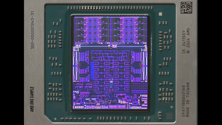
Before we dive into the report, it’s essential to acknowledge the work by High Yield made to discover the change in D2D interconnect with Strix Halo, and it’s really an exciting discovery. Now, as AMD, you can rely on process advancements, revamping chiplet designs, and other elements to squeeze out more performance, but when it comes to D2D (die-to-die) interconnects, Team Red has been on the same technology since Zen 2. However, with next-gen Zen 6 processors, this could change, and interestingly, ‘Zen 6 DNA’ is found in the Strix Halo APUs.
Let’s discuss how the current interconnect works. To communicate between dies, AMD leverages the ‘SERDES PHYs’ on the CCD edge dies. These allow high‑speed serial lanes to communicate across the organic substrate to an I/O/SoC die. SERDES represents a serializer/deserializer, and it is primarily used to convert parallel traffic coming from individual CCDs to serial bitstreams and launch them across the package since using hundreds of copper wires between dies is not practical on a conventional substrate alone.
On the other end, the deserializer converted the serial bitstreams back to the fabric on the other side. Now, if you guessed why SERDES is a bit of an inefficient approach, you are spot-on, but if not, the overhead required with serializing/deserializing utilizes energy for clock recovery, equalization, and encoding/decoding. Secondly, converting data streams also adds latency between D2D communication on both ends, which is also a drawback of the current approach.
The SERDES approach was good enough when D2D communication was limited to certain ‘traditional’ dies, but with the addition of NPUs, firms like AMD need steady, low-overhead bandwidth to memory and the CCDs. Now, essentially with Strix Halo, Team Red has revamped the way Zen 6 dies could communicate. This is done through TSMC’s InFO-oS (Integrated Fan-Out on Substrate) along with a redistribution layer (RDL), and we’ll explain how both work in depth next.
To cater to the overhead involved in converting data streams, what AMD did with Strix Halo is lay out several short, skinny parallel wires between the dies that live in the ‘interposer’ under the dies made from RDL. Through InFO-oS, the manufacturer laid out the cables between the silicon dies and the organic substrate, and now, the CPU fabric communicates across wide parallel ports. If you ask how High Yield figured out the new approach, Strix Halo has a rectangular field of tiny pads, which is a classical representation of a ‘fan out’ implementation, and the big ‘SERDES’ block was removed.
Now with the newer approach, both power and latency requirements are reduced since there’s no serializing/deserializing, and more importantly, the overall bandwidth scales up by adding higher ports across the CPU fabric. However, there are complications with the fan-out approach, particularly with the design complexities involved in multi-layer RDL, and routing priorities now also need to change since the under-die space is busy with fan-out wiring.
Either way, it’s amazing to witness what AMD has brought with Strix Halo in terms of D2D interconnect, and its approach is expected to remain consistent with Zen 6 CPUs. Yet again, High Yield made an amazing discovery; hence, make sure to check the channel out.