Copyright scmp
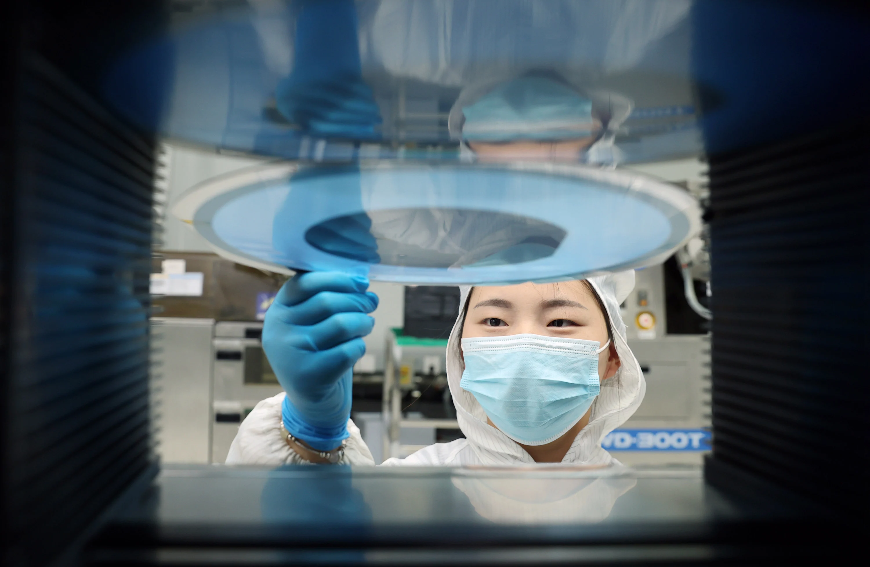
In a major leap for the global semiconductor industry, a joint Chinese research team has developed a method that can slash defects in lithography – a critical step in chipmaking – by up to 99 per cent. The researchers achieved unprecedented clarity by using cryo-electron tomography (cryo-ET) to pinpoint, for the first time, the minute sources of common manufacturing flaws. The findings, published in the journal Nature Communications on September 30, by Professor Peng Hailin from Peking University in collaboration with researchers from Tsinghua University and the University of Hong Kong, were hailed by reviewers as a “fancy tool” that “would benefit peer researchers and industrial users quite a lot”. “The team has proposed a solution compatible with existing semiconductor production lines,” Peng said in an interview with Beijing-based Science and Technology Daily published on Monday. “It can reduce lithography defects on 12-inch (30cm) wafers by 99 per cent,” he added, indicating substantial cost benefits to the market. Lithography is one of the most critical steps in chip manufacturing. “It can be understood as ‘printing circuits’ onto semiconductor wafers such as silicon,” Peng said. “Essentially, an ultra-precise ‘projector’ shrinks and transfers pre-designed circuit patterns onto a special film coating the wafer, which is then developed and fixed.” For instance, during the etching process for silicon chips, photoresist – a light-sensitive material – functions in three stages. First, liquid photoresist is evenly applied to the wafer surface. Next, a lithography machine projects ultraviolet or extreme ultraviolet light through a mask with circuit patterns to expose the photoresist. During the final stage – development, which is key to revealing the circuit pattern – the exposed photoresist undergoes chemical changes, making it more or less soluble. Developer is then used to wash away soluble areas, leaving a patterned photoresist layer that acts as a protective mask. This layer determines the formation of complex circuits in subsequent etching and ion implantation processes. This is where problems tend to occur. During development, dissolved photoresist molecules can readhere and become entangled, forming large particles. These particles may redeposit onto delicate circuit patterns, causing critical defects such as “bridging”. In their analysis, Peng’s team found that the number of defects on a single 12-inch wafer could exceed 6,600 – unacceptable for mass production. Until now, the development process has largely been a black box for manufacturers, forcing them to rely on time-consuming and costly trial-and-error optimisations. As process nodes shrink to 5 nanometres, agglomerated particles as small as 30nm can cause excessive line-edge roughness, potentially leading to tens of millions of dollars in losses. To address the challenge, the team was the first to introduce cryo-ET into semiconductor research. After the usual lithography steps, they instantaneously froze the thin layer of developer containing photoresist to minus 175 degrees Celsius (minus 283 Fahrenheit), vitrifying it and effectively freezing the molecular conformations in time. The researchers then performed three-dimensional reconstruction using multi-angle imaging, allowing direct observation of the behaviour of the photoresist molecules in the developer. For the first time, the team could see entanglement among photoresist polymer chains. Adsorbed chains formed “loose entanglements” via weak hydrophobic interactions, eventually agglomerating into particles measuring 30 to 40nm. They also noticed about 70 per cent of the polymers were not dissolved in the liquid but adsorbed at the air-liquid interface. These particles later redeposited during rinsing, becoming the main cause of pattern defects. Based on these insights, the team proposed a dual-approach strategy compatible with existing semiconductor production lines. First, to suppress entanglement, they moderately increased the post-exposure bake temperature, effectively reducing polymer entanglement and significantly minimising the formation of large aggregates at the source. Second, they optimised the development process to trap polymers at the air-liquid interface, allowing them to be completely carried away with fluid flow and preventing redeposition onto the patterned surface. “Tests have confirmed that pattern defects caused by photoresist residues on 12-inch wafers were successfully eliminated, with defect counts reduced by more than 99 per cent,” Science and Technology Daily quoted Peng as saying. “The solution also demonstrated high reliability and repeatability.” A report by Beijing-based consulting firm QY Research in March indicated that the global photoresist market had reached US$6.3 billion in 2024 and was expected to grow at a compound annual growth rate of around 6.7 per cent, reaching US$10 billion by 2030. According to an analysis by industry information portal Elecfans, although photoresist accounts for only about 5 per cent of chip material costs, its performance directly affects chip yield, so manufacturers are less sensitive to price and more concerned with stability. The global photoresist industry is highly consolidated, with the top five suppliers – mainly from Japan, the United States and South Korea – dominating about 90 per cent of the market. This breakthrough could change that, allowing China to enter the high-end photoresist sector. Cryo-ET technology could also drive improvements in other areas of chip manufacturing, helping to improve quality control and yield in key processes such as lithography, etching and wet cleaning in advanced nodes, Peng said.